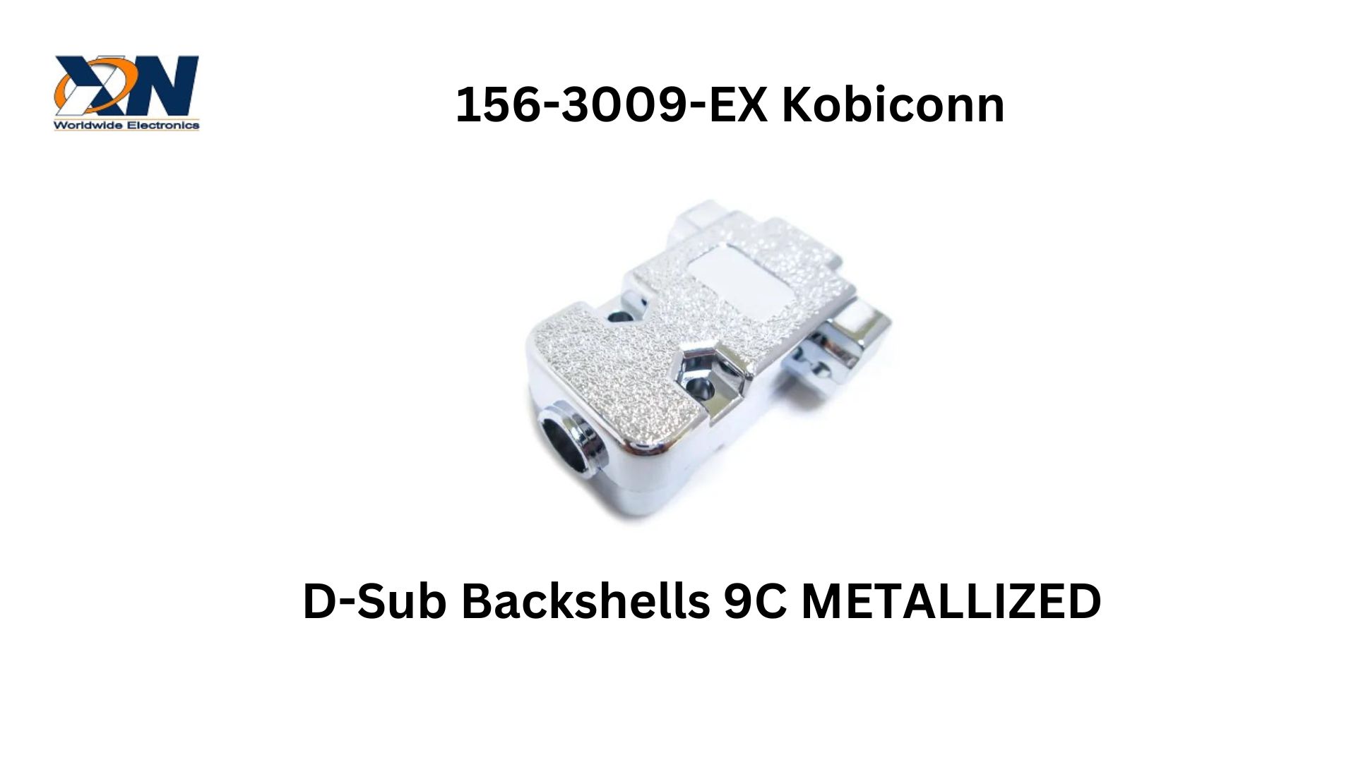
 156-3009-EX D-Sub Backshells Retailer in USA 156-3009-EX D-Sub Backshells Retailer in USA Sep 6, 2024
Xon Electronic is the leading global retailer of the 156-3009-EX D-Sub Backshell, manufactured by Kobiconn. Designed for 9-pin D-Sub connectors, this metallized backshell provides superior EMI/RFI shielding, ensuring reliable performance in industrial, medical, and telecommunications applications. | 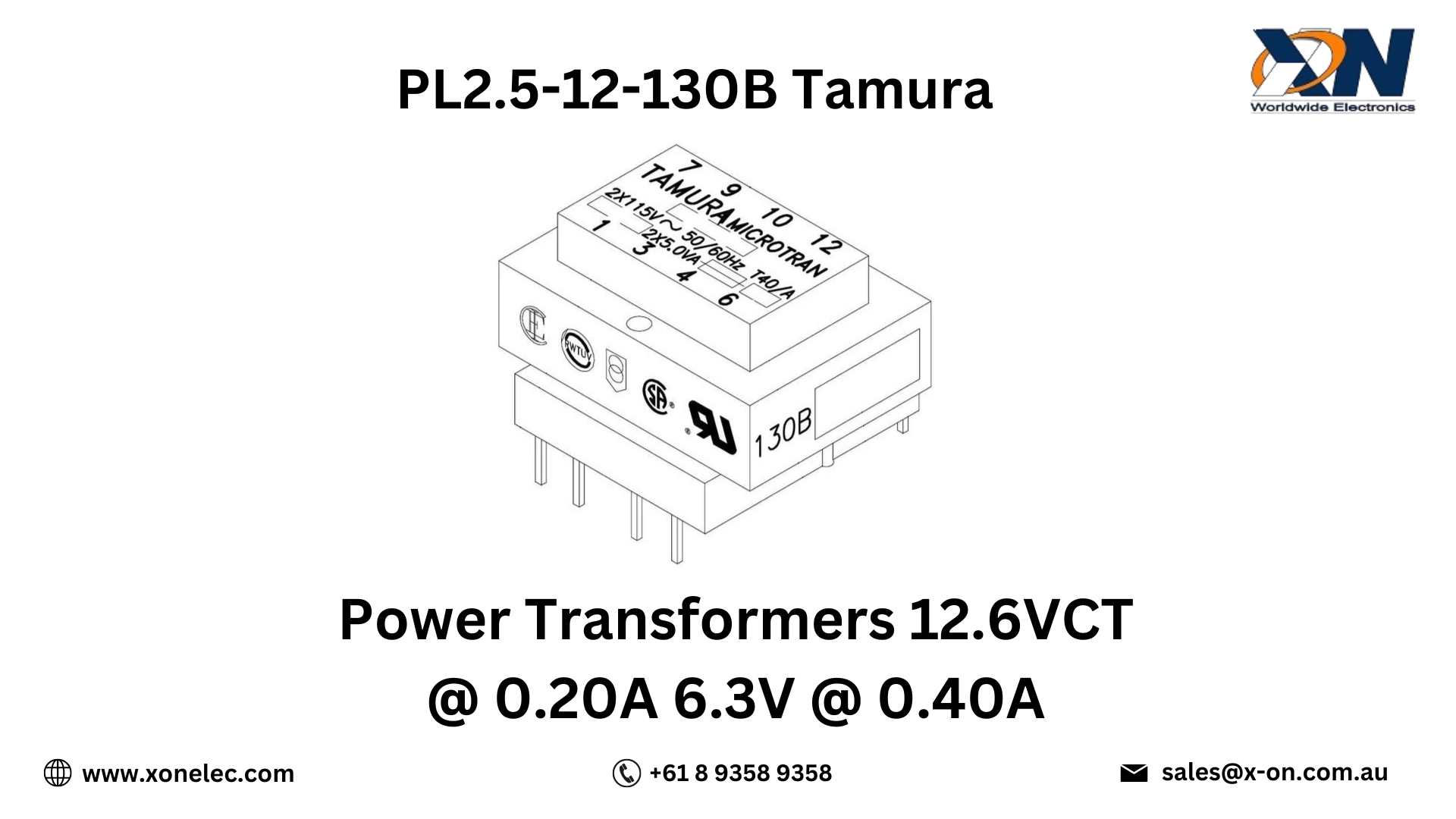 Best PL2.5-12-130B Power Transformers Retailer in India, USA Best PL2.5-12-130B Power Transformers Retailer in India, USA Sep 22, 2024
Discover the PL2.5-12-130B Power Transformer by Tamura, available at Xon Electronic, a global leader in electronic component retail. With 12.6VCT at 0.20A and 6.3V at 0.40A outputs, this transformer is ideal for consumer electronics, prototyping, and educational projects. Xon Electronic offers fast | 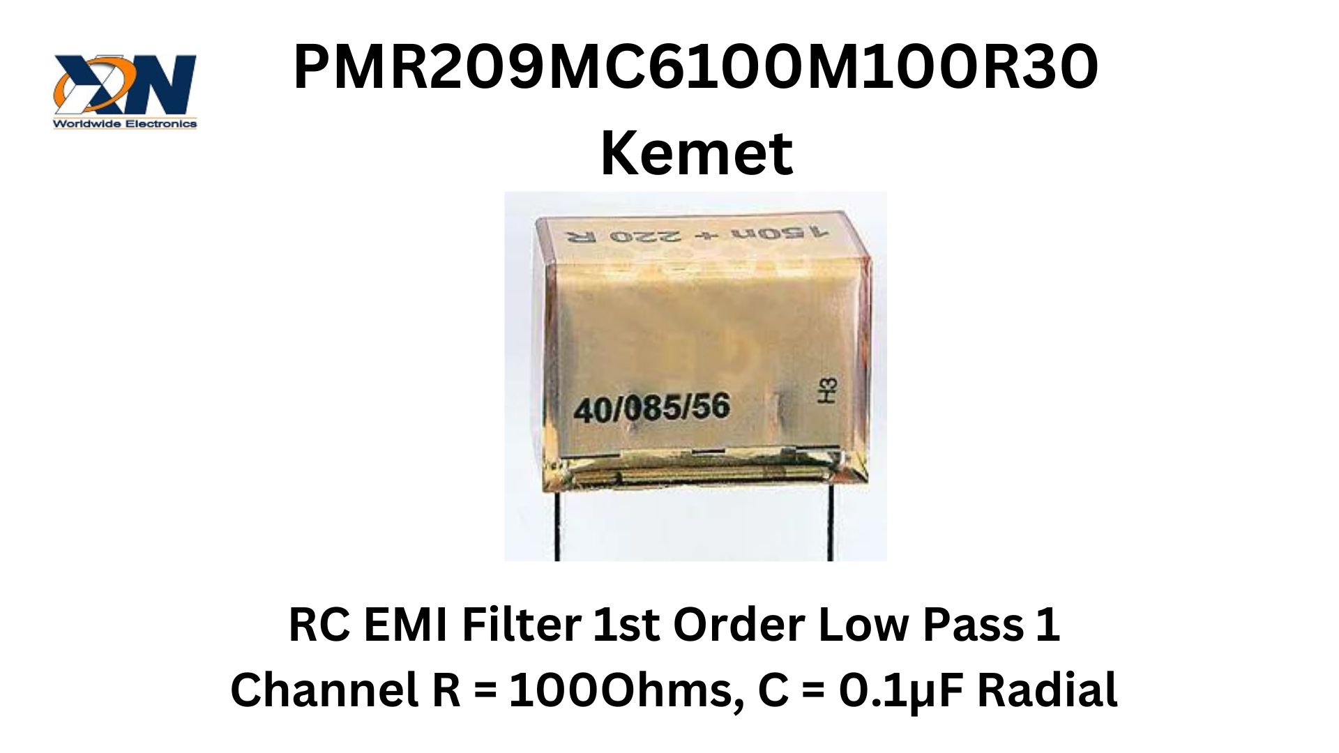 PMR209MC6100M100R30 Film Capacitors Retailer in India, USA, Australia PMR209MC6100M100R30 Film Capacitors Retailer in India, USA, Australia Aug 5, 2024
Discover why X-ON Worldwide Electronics is the best retailer for PMR209MC6100M100R30 film capacitors, manufactured by Kemet. Offering high stability, low loss, and exceptional performance, these capacitors are ideal for power supplies, signal processing, and industrial automation. Explore the detai | 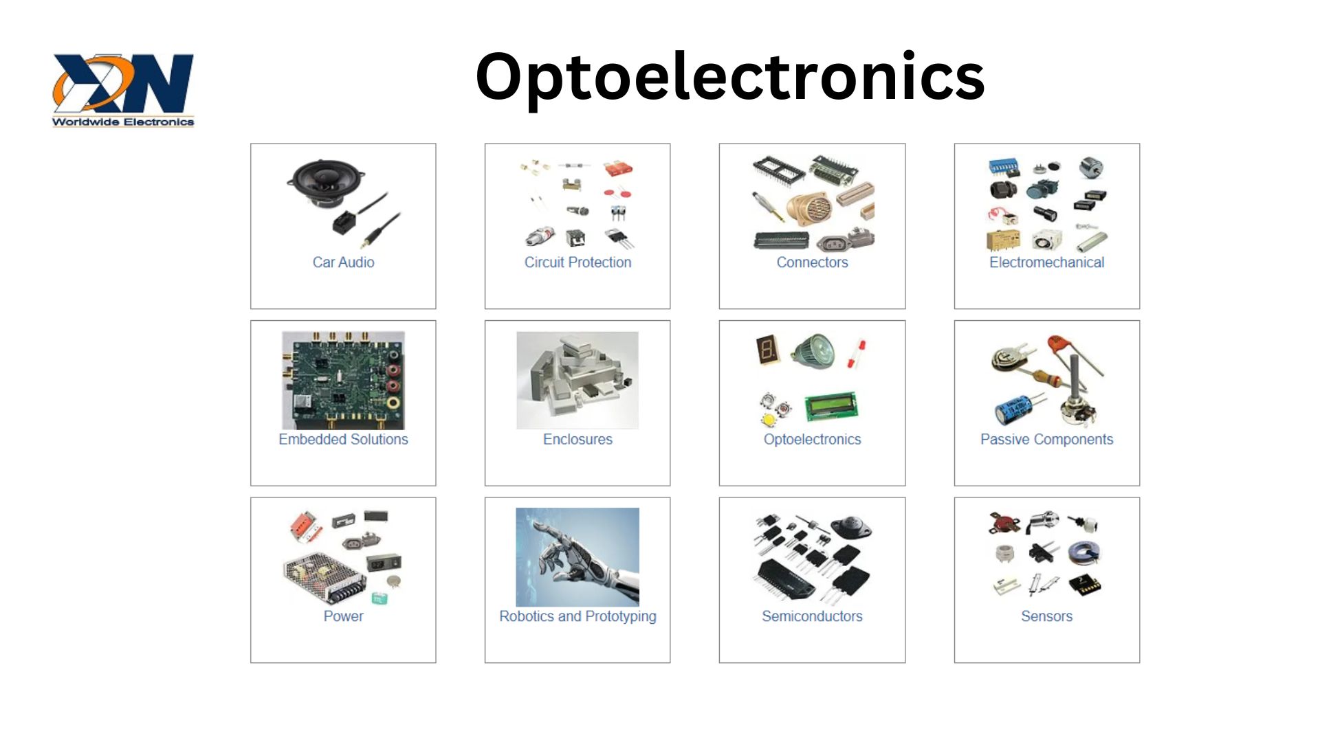 Understanding Optoelectronics: A Comprehensive Guide Understanding Optoelectronics: A Comprehensive Guide Jul 9, 2024
Optoelectronics, a fascinating and rapidly advancing field, combines the principles of optics and electronics to create devices that source, detect, and control light. This comprehensive guide delves into the fundamentals of optoelectronics, covering key components like LEDs, photodiodes, and lasers |