 Best 0154005.DRT Surface Mount Fuses Retailer and Wholesalers
 Oct 4, 2024
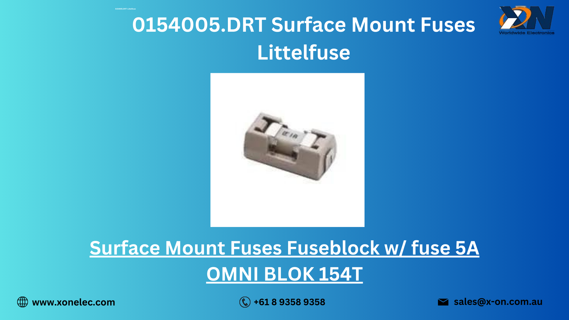
Looking for the best retailer and wholesaler of the 0154005.DRT Surface Mount Fuse ? Xon Electronic is your trusted global supplier, offering Littelfuse's OMNI-BLOK 154T series 5A fuse . With fast shipping to the USA, India, Australia, Europe, and more, Xon Electronic ensures high-quality, reliab