X-On Electronics has gained recognition as a prominent supplier of W29N01GWDIBA NAND Flash across the USA, India, Europe, Australia, and various other global locations. W29N01GWDIBA NAND Flash are a product manufactured by Winbond. We provide cost-effective solutions for NAND Flash, ensuring timely deliveries around the world.

W29N01GWDIBA Winbond

W29N01GWDIBA electronic component of Winbond
Product Image X-ON
Product Image X-ON
Product Image X-ON

Images are for reference only
See Product Specifications
Part No.W29N01GWDIBA
Manufacturer: Winbond
Category: NAND Flash
Description: NAND Flash 1G-bit NAND flash, 1.8V, 1-bit ECC, 3V, x16
Datasheet: W29N01GWDIBA Datasheet (PDF)
This product is classified as Large/Heavy, additional shipping charges may apply. A customer service representative may contact you after ordering to confirm exact shipping charges


Price (USD)
1: USD 1.2451 ea
Line Total: USD 1.25 
Availability - 248
Ship by Thu. 07 Nov to Wed. 13 Nov
MOQ: 1  Multiples: 1
Pack Size: 1
Availability Price Quantity
248
Ship by Thu. 07 Nov to Wed. 13 Nov
MOQ : 1
Multiples : 1
1 : USD 1.2451
10 : USD 1.2254
25 : USD 1.2056
100 : USD 1.1857
250 : USD 1.1658

   
Manufacturer
Product Category
LoadingGif
 
Notes:- Show Stocked Products With Similar Attributes.

We are delighted to provide the W29N01GWDIBA from our NAND Flash category, at competitive rates not only in the United States, Australia, and India, but also across Europe and beyond. A long established and extensive electronic component distribution network has enhanced our global reach and dependability, ensuring cost savings through prompt deliveries worldwide. Client satisfaction is at the heart of our business, where every component counts and every customer matters. Our technical service team is ready to assist you. From product selection to after-sales support, we strive to deliver a seamless and satisfying experience. Are you ready to experience the best in electronic component distribution? Contact X-ON Electronics today and discover why X-On are a preferred choice for the W29N01GWDIBA and other electronic components in the NAND Flash category and beyond.

Image Part-Description
Stock Image W29N01HVSINF
NAND Flash 1G-bit NAND flash, 3V, 4-bit ECC, 3V, x8
Stock : 0
This product is classified as Large/Heavy, additional shipping charges may apply. A customer service representative may contact you after ordering to confirm exact shipping charges.
Stock Image W29N01HVDINF
NAND Flash 1G-bit NAND flash, 3V, 4-bit ECC, 3V, x8
Stock : 0
This product is classified as Large/Heavy, additional shipping charges may apply. A customer service representative may contact you after ordering to confirm exact shipping charges.
Stock Image W29N01GZDIBA
NAND Flash 1G-bit NAND flash, 1.8V, 1-bit ECC, 3V, x8
Stock : 0
This product is classified as Large/Heavy, additional shipping charges may apply. A customer service representative may contact you after ordering to confirm exact shipping charges.
Stock Image W29N01HZBINF
NAND Flash 1G-bit NAND flash, 1.8V, 4-bit ECC x8
Stock : 0
This product is classified as Large/Heavy, additional shipping charges may apply. A customer service representative may contact you after ordering to confirm exact shipping charges.
Stock Image W29N01HVBINF
NAND Flash 1G-bit NAND flash, 3V, 4-bit ECC, 3V, x8
Stock : 124
This product is classified as Large/Heavy, additional shipping charges may apply. A customer service representative may contact you after ordering to confirm exact shipping charges.
Stock Image W29N01HVBINA
NAND Flash 1G-bit NAND flash, 3V, 1-bit ECC, 3V, x8
Stock : 0
This product is classified as Large/Heavy, additional shipping charges may apply. A customer service representative may contact you after ordering to confirm exact shipping charges.
Stock Image W29N01HVSINA
NAND Flash 1G-bit NAND flash, 3V, 1-bit ECC, 3V, x8
Stock : 945
This product is classified as Large/Heavy, additional shipping charges may apply. A customer service representative may contact you after ordering to confirm exact shipping charges.
Stock Image W29N01HVDINA
NAND Flash 1G-bit NAND flash 3V 1-bit ECC 3V x8
Stock : 100
This product is classified as Large/Heavy, additional shipping charges may apply. A customer service representative may contact you after ordering to confirm exact shipping charges.
Stock Image W29N01HZBINA
NAND Flash 1G-bit NAND flash 1.8V 1-bit ECC x8
Stock : 0
This product is classified as Large/Heavy, additional shipping charges may apply. A customer service representative may contact you after ordering to confirm exact shipping charges.
Stock Image W29N01HZDINA
NAND Flash 1G-bit NAND flash 1.8V 1-bit ECC x8
Stock : 0
This product is classified as Large/Heavy, additional shipping charges may apply. A customer service representative may contact you after ordering to confirm exact shipping charges.
Image Part-Description
Stock Image W29N01GZDIBA
NAND Flash 1G-bit NAND flash, 1.8V, 1-bit ECC, 3V, x8
Stock : 0
This product is classified as Large/Heavy, additional shipping charges may apply. A customer service representative may contact you after ordering to confirm exact shipping charges.
Stock Image XC7SHU04GV
IC, INVERTER, SC-74A
Stock : 0
This product is classified as Large/Heavy, additional shipping charges may apply. A customer service representative may contact you after ordering to confirm exact shipping charges.
Stock Image W29N04GVSIAA
NAND Flash 4G-bit NAND flash, 3V x 8bit
Stock : 0
This product is classified as Large/Heavy, additional shipping charges may apply. A customer service representative may contact you after ordering to confirm exact shipping charges.
Stock Image XC7VX485T-2FFG1761C
FPGA Virtex-7 XT Family 485760 Cells 28nm Technology 1V 1761-Pin FCBGA
Stock : 0
This product is classified as Large/Heavy, additional shipping charges may apply. A customer service representative may contact you after ordering to confirm exact shipping charges.
Stock Image XC7WT14GD
IC, INV, SCHMITT TRIGGER, XSON8U
Stock : 0
This product is classified as Large/Heavy, additional shipping charges may apply. A customer service representative may contact you after ordering to confirm exact shipping charges.
Stock Image XC7Z010-L1CLG400I
FPGA Zynq-7000 28000 Cells 28nm Technology 1V 400-Pin CS-BGA
Stock : 0
This product is classified as Large/Heavy, additional shipping charges may apply. A customer service representative may contact you after ordering to confirm exact shipping charges.
Stock Image XC7Z015-2CLG485E
MPU Zynq-7000 RISC 32-Bit 766MHz 1.5V/2V/2.5V 485-Pin CSBGA
Stock : 0
This product is classified as Large/Heavy, additional shipping charges may apply. A customer service representative may contact you after ordering to confirm exact shipping charges.
Stock Image XC7Z020-1CLG400I
MPU Zynq-7000 Thumb-2 32-Bit 667MHz 1.2V/3.3V 400-Pin CS-BGA
Stock : 44
This product is classified as Large/Heavy, additional shipping charges may apply. A customer service representative may contact you after ordering to confirm exact shipping charges.
Stock Image XC7Z020-2CLG400E
MPU Zynq-7000 Thumb-2 32-Bit 733MHz 1.2V/3.3V 400-Pin CS-BGA
Stock : 0
This product is classified as Large/Heavy, additional shipping charges may apply. A customer service representative may contact you after ordering to confirm exact shipping charges.
Stock Image XC7Z020-L1CLG400I
FPGA Zynq-7000 85000 Cells 28nm Technology 1V 400-Pin CS-BGA
Stock : 2
This product is classified as Large/Heavy, additional shipping charges may apply. A customer service representative may contact you after ordering to confirm exact shipping charges.

W29N01GZ/W W29N01GZ/W 1G-BIT 1.8V NAND FLASH MEMORY th Release Date: January 11 , 2018 1 Revision J W29N01GZ/W Table of Contents 1. GENERAL DESCRIPTION ............................................................................................................... 7 2. FEATURES ....................................................................................................................................... 7 3. PACKAGE TYPES AND PIN CONFIGURATIONS .......................................................................... 8 3.1 Pin assignment 48 ball VFBGA X8/X16 ......................................................................... 8 3.2 Pin Descriptions .................................................................................................................... 9 4. PIN DESCRIPTIONS ...................................................................................................................... 10 4.1 Chip Enable ( CE) .............................................................................................................. 10 4.2 Write Enable ( WE) ............................................................................................................ 10 4.3 Read Enable ( RE) ............................................................................................................ 10 4.4 Address Latch Enable (ALE) .............................................................................................. 10 4.5 Command Latch Enable (CLE) .......................................................................................... 10 4.6 Write Protect ( WP) ............................................................................................................ 10 4.7 Ready/Busy (RY/ BY) ........................................................................................................ 10 4.8 Input and Output (I/Ox) ....................................................................................................... 10 5. BLOCK DIAGRAM .......................................................................................................................... 11 6. MEMORY ARRAY ORGANIZATION .............................................................................................. 12 6.1 X8 Array Organization ........................................................................................................ 12 6.2 X16 Array Organization ...................................................................................................... 13 7. MODE SELECTION TABLE ........................................................................................................... 14 8. COMMAND TABLE......................................................................................................................... 15 9. DEVICE OPERATIONS .................................................................................................................. 16 9.1 READ operation .................................................................................................................. 16 9.1.1 PAGE READ (00h-30h)......................................................................................................... 16 9.1.2 CACHE READ OPERATIONS .............................................................................................. 17 9.1.3 RANDOM DATA OUTPUT (05h-E0h) ................................................................................... 21 9.1.4 READ ID (90h) ...................................................................................................................... 22 9.1.5 READ PARAMETER PAGE (ECh) ....................................................................................... 23 9.1.6 READ STATUS (70h)............................................................................................................ 25 9.1.7 READ UNIQUE ID (EDh) ...................................................................................................... 27 9.2 PROGRAM operation ......................................................................................................... 28 9.2.1 PAGE PROGRAM (80h-10h) ................................................................................................ 28 9.2.2 SERIAL DATA INPUT (80h) .................................................................................................. 28 9.2.3 RANDOM DATA INPUT (85h) .............................................................................................. 29 9.2.4 CACHE PROGRAM (80h-15h) ............................................................................................. 29 9.3 COPY BACK operation....................................................................................................... 31 9.3.1 READ for COPY BACK (00h-35h) ........................................................................................ 31 9.3.2 PROGRAM for COPY BACK (85h-10h) ................................................................................ 31 9.4 BLOCK ERASE operation .................................................................................................. 33 9.4.1 BLOCK ERASE (60h-D0h) .................................................................................................... 33 9.5 RESET operation ................................................................................................................ 34 9.5.1 RESET (FFh) ........................................................................................................................ 34 9.6 FEATURE OPERATION..................................................................................................... 35 th Release Date: January 11 , 2018 2 Revision J

Tariff Desc

8542.32.00 32 No ..CMOS and MOS Read Only Memory and Programmable Read Only Memory whether erasable or non-erasable (for example, flash memory, EPROM, E2PROM, EAPROM, NOVRAM, ROM and PROM)
WINBOND ELECTRONICS
WINBOND ELECTRONICS CORP AMERICA
Best 1172C SL001 Multi-Conductor Cables Retailer in India image

Oct 14, 2024
The 1172C SL001 Multi-Conductor Cable by Alpha Wire is a 22 AWG, 2-conductor unshielded cable designed for low-voltage applications such as control circuits, data communication, and security systems. Encased in a durable PVC jacket, it provides excellent resistance to chemicals, moisture, and wear.
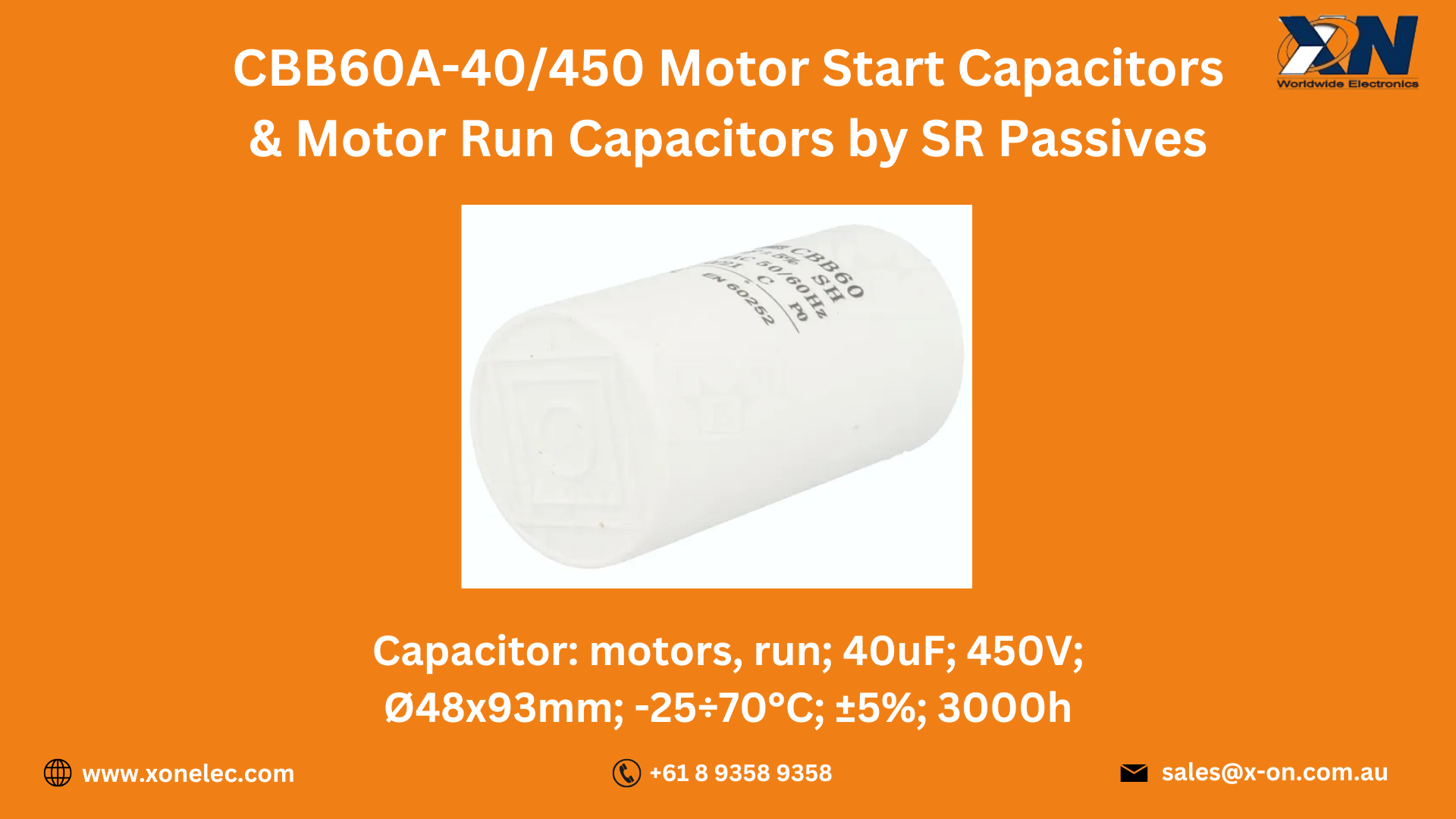
CBB60A-40/450 SR Passives Motor Start and Run Capacitors image

Oct 30, 2024
Explore the versatile CBB60A-40/450 SR Passives Motor Start and Run Capacitors, engineered to enhance motor performance in both industrial and domestic applications across the USA, India, Australia, Europe, and beyond. With a 40µF capacitance, 450V rating, and temperature resilience from -25°C to 7
Transistors and Resistors and its Difference: The Heart of Electronic Devices image

Jul 3, 2024

Transistors and resistors are fundamental components in the world of electronics, each serving unique and crucial roles in circuit design and functionality. Understanding their differences and applications is essential for anyone involved in elec

Supplier of the E-TDA7377 Audio Amplifier in USA, India, Australia image

Jul 8, 2024

Xon Electronics has distinguished itself as a premier supplier of the E-TDA7377, a highly sought-after audio amplifier IC manufactured by STMicroelectronics. With a strong presence in the USA, India,

Looking for help? Visit our FAQ's Section to answer to all your questions


X-ON Worldwide Electronics

Welcome To X-ON Electronics
For over three decades, we have been advocating and shaping the electronic components industry. Our management complements our worldwide business scope and focus. We are committed to innovation, backed by a strong business foundation. If you need a trustworthy supplier of electronic components for your business – look no further.
 

Copyright ©2024  X-ON Electronic Services. All rights reserved.
Please ensure you have read and understood our Terms & Conditions before purchasing. All prices exclude GST.

Image for all the cards that are accepted Image for all the cards that are accepted Image for all the cards that are accepted Image for all the cards that are accepted Image for all the cards that are accepted AS9120 Certified